Characterization of microstructures
MEMS-characterization by laser interferometric systems
Traditional measuring systems reach their limits when characterizing microstructures. One solution is to use a laser vibrometer in combination with a technical microscope and the nanopositioning and nanomeasuring machine from SIOS Messtechnik. This set-up enables movements and surfaces of objects to be measured to a resolution of 0.1 nanometers.
Micro-electromechanical systems (MEMS) are devices or machines consisting of both electrical and mechanical components which work together as a system. Their measurements typically lie in the micrometer range. Examples of micro-electromechanical systems are: AFM cantilevers, pressure sensors, acceleration sensors, printheads in inkjet printers, mechanical image stabilizers in digital cameras, and sensor chips for use in pharmacy, biology and chemistry.
In order to ensure high quality standards, comprehensive characterization is essential throughout the entire development and production processes. This involves determining a number of parameters. These include dynamic characteristic values, such as resonance frequencies of vibrating structures and their modes of vibration, as well as static variables, such as the topography of a surface and values derived from it, examples of this being structure heights and depths, deflections of membranes and roughness values.
As a result of continuing technical development, ever smaller structure widths are also establishing themselves in the microengineering field. This is where traditional measuring systems, such as tactile profilometers, reach their limits. They are unable to guarantee the required spacial resolution in the submicrometer range. Moreover, the pressure of the probe tip may damage or destroy the measured object.
This is where laserinterferometric measuring processes offer a solution. For example, a laser vibrometer from SIOS Messtechnik GmbH used in conjunction with a technical microscope can measure dynamic characteristics precisely and without physical contact. The nanopositioning and nanomeasuring machine together with various scanning systems can determine the topography of such a system with extreme precision.
Vibration analysis of microstructures
Laserinterferometric processes are suitable for measuring vibrations because they guarantee high precision, and the measurement results can be traced back to the international standards of measurement.
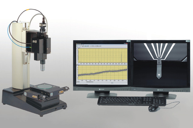
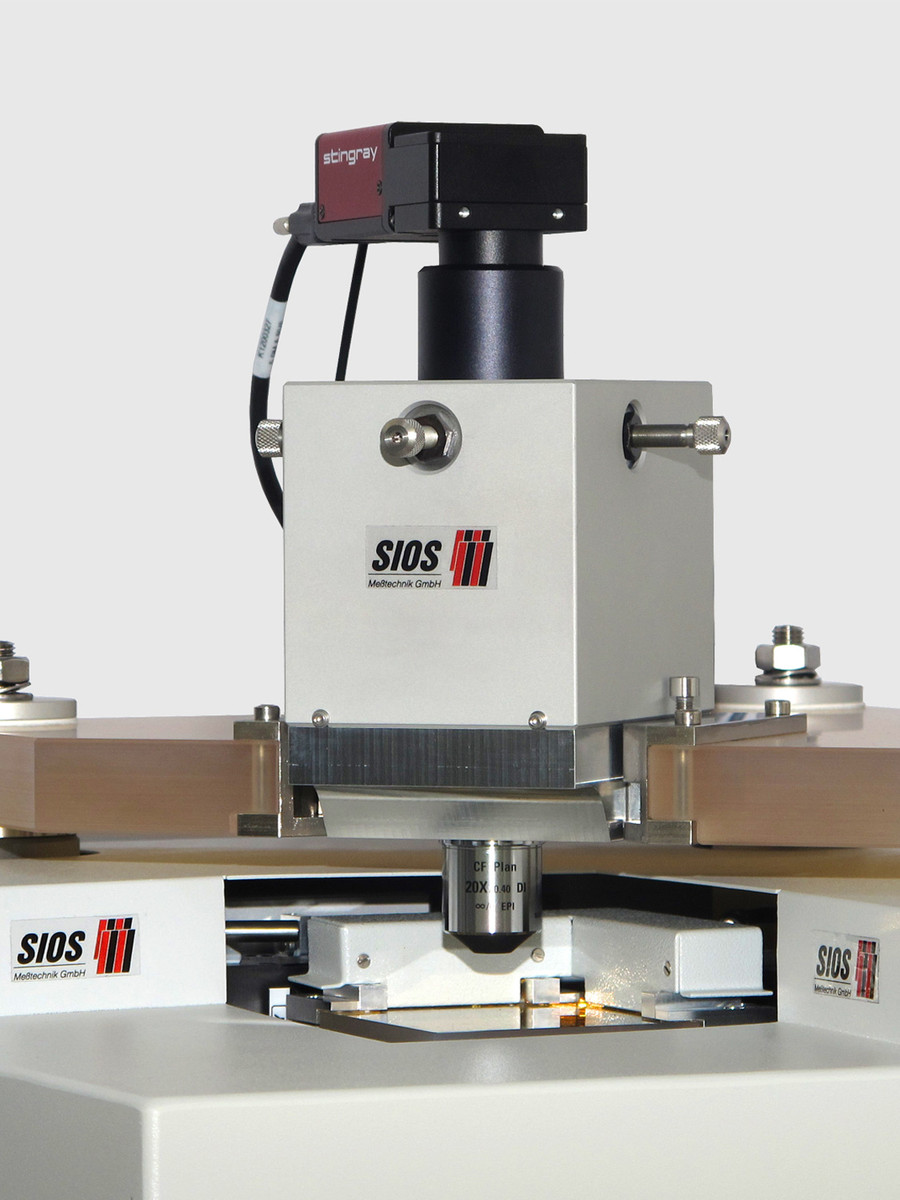
The nano vibration analyzer NA works without contact, and consists of a laserinterferometric vibrometer and a technical microscope. It is used for the non-contact vibration analysis of MEMS and microstructures.
The heart of the vibrometer is a Michelson interferometer. The optical-fiber coupling allows the use of a relatively small sensor, which is free from the thermal influence of the laser. Used in conjunction a technical microscope, it forms a high-performance set-up for measuring the lengths and vibrations of MEMS, micro-objects and cantilevers.
This device is characterized by a distance resolution of 5 pm and a frequency measuring range from 0 to 5 MHz. Interchangeable lenses enable the laser spot diameter and the working distance to the lense to be adjusted. For example, the laser spot diameter of a 50x objective is < 2 μm. A positioning table with a 50 mm x 50 mm traversing area enables an object to be scanned. The object measured can be observed through the integrated USB camera.
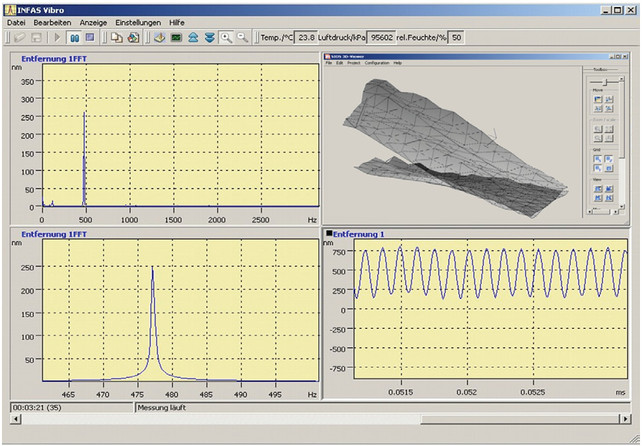
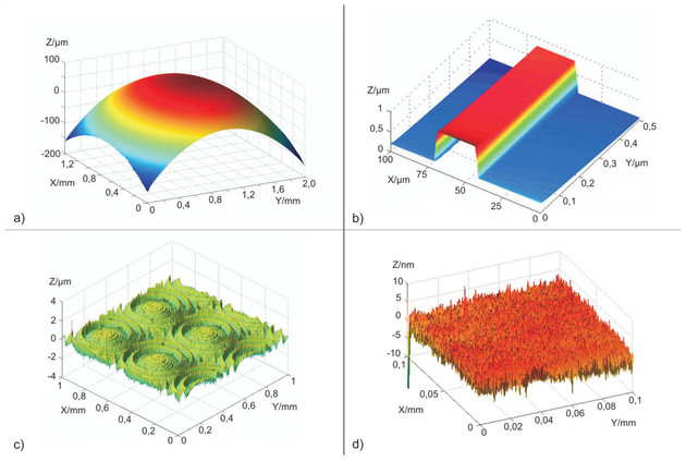
Special software enables the script-controlled scanning of the measured object. In addition it provides the possibility of spectral analysis and averaging of the measurement data. The velocity and acceleration of the vibration can be calculated, and the surface vibration can be displayed in 3D.
Analysis of the surface topography
The nanopositioning and nanomeasuring machine NMM-1 is an all-purpose device for analyzing the surface topography of microstructures and MEMS.
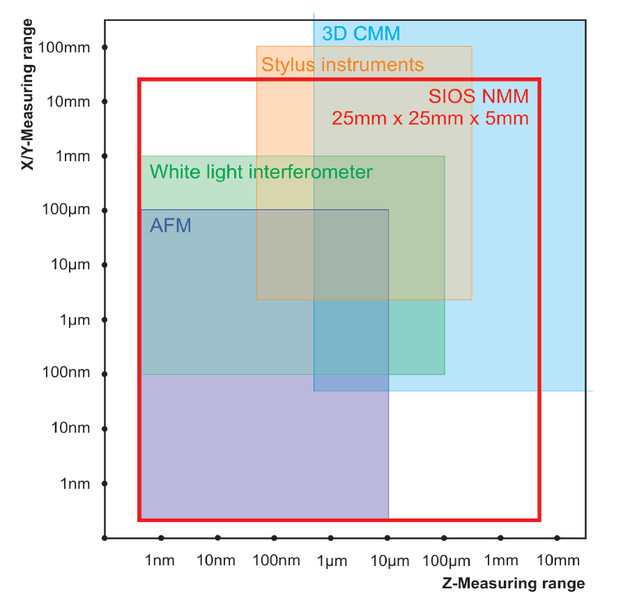
The high resolution of 0.1 nm in a measuring range of 25 mm x 25 mm x 5 mm together with optional integration of various scanning systems enable 2D and 3D measurements to be made over a very large measuring area.
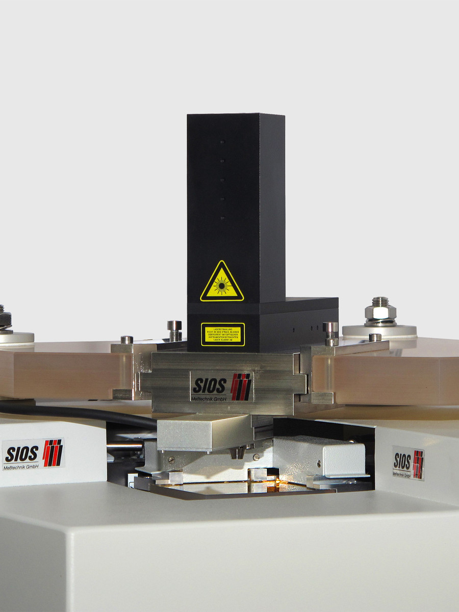
The precision of the nanopositioning and nanomeasuring machine is based on the arrangement of the three laser interferometers for position measurement. The three measuring beams meet at the same point where the scanning system has its measuring point. This maintains the Abbe comparator principle in all three measuring axes. The scanning system serves as a zero-point indicator within the nanopositioning and nanomeasuring machine. This additionally maintains the Abbe comparator principle throughout the measurement. Optical and tactile scanning systems each have different characteristics and fields of application. Therefore it is important to select the best scanning system a particular measuring task. All the scanning systems used have high reproducibility and can be exchanged and mounted on the metrological frame of the nanopositioning and nanomeasuring machine using a simple adapter. The analog interface of the machine is open for the use of other, newer scanning systems.
The following scanning systems are currently integrated into the nanopositioning and nanomeasuring machine:
Fix focus sensor

Atomic force microscope
White light sensor

Tactile 3D sensor
These enable the machine to be used a diverse range of applications, such as positioning, manipulating, processing and measuring objects in fields such as microelectronics, micromechanics, optics and microsystem engineering.
Measurement uncertainties as low as in the subnanometer range can be achieved. The measuring range of these high-resolution measuring systems can be extended by using them in conjunction with a scanning probe microscope. The nanopositioning and nanomeasuring machine is therefore an all-purpose device for 2D and 3D measurement of MEMS and micro-objects.

Situable products and solutions


Nanopositioning and Nanomeasuring Machine
high accuracy nanopositioning and measuring system